For half a century, the rapid evolution of information technology has been described by a trend known as Moore’s Law: the number of transistors in integrated circuits doubles every two years or so. However, silicon based transistors are fast approaching their size limits, forcing researchers to look for alternative technologies. A team led by ZHANG Yue, a professor of Materials Science and Engineering at the University of Science and Technology Beijing (USTB) and an Academician of the Chinese Academy of Science, has been examining atomically thin material candidates as a way to fit more transistors on a chip.
Despite exponential development for decades, conventional silicon semiconductors, materials are used to make transistors, are reaching the edge of their capacity. Chips keep shrinking, and the performance of conventional semiconductors declines significantly at the sub-5 nanometre scale. Another issue is the chemical bond, integral for mixing different materials, including semiconductors, oxide materials and metals, to make a transistor. Only limited types of materials can be chemically bonded to form a heterostructure, a combination of multiple dissimilar materials. This approach can cause defects that reduce the efficiency of electron transport, which is exacerbated by the shrinking size of transistors.
“Imagine 100 kids are hand in hand, trying to form a 10 by 10 array. While some of them are much slimmer than others, it won’t be easy to bring them in alignment. You can ask the slimmer kids to keep a wider distance from others, but it will be much harder when they are getting really close,” says ZHANG Zheng, a material scientist at USTB and a member of ZHANG Yue’s team. “That’s what happens with atoms when mixing different materials in conventional ways.”
Thinner and flatter
For ZHANG Yue and his colleagues, one of the promising solutions is two dimensional (2D) materials. These ultrathin materials, which can be only 0.6 nanometres thick for one-layer 2D compounds, have shown similar carrier mobility to bulk silicon, with atomically flat and dangling-bond free surface that allow carriers to flow relatively smoothly through them. This kind of material allows the fabrication of integrated circuits closer to one nanometre.
Instead of chemical bonding, ZHANG Yue and his colleagues are exploring the approach of stacking atom layers using van der Waals (vdW) force to form heterostructures.
“Using Van der Waals force is like making these 2D compounds combined back to back. You don’t have to worry about whether their chemical bond connected together or not,” says ZHANG Zheng. This has provided great flexibility to integrate distinct atomic layers beyond the traditional limits of lattice-matching requirements.
This approach has proven fruitful. In 2021, by stacking the 2D metal ― a metallic phase molybdenum ditelluride ― and the semiconducting monolayer, molybdenum disulfide, using vdW force, the team reported a near-ideal Schottky diode, a semiconductor diode formed by the junction of a semiconductor with a metal.
However, it is much more challenging to prepare high-order vdW superlattices with a larger number of alternating materials by mechanical restacking or sequential synthesis, because of material damage associated with each sequential restacking or synthesis step. To address this, the team worked with both local and international researchers, and developed a new strategy of “rolling up” van der Waals heterostructures. As ZHANG Zheng explains, “as the atoms don’t have to ‘hold hands’, two types of vdW integrated 2D materials can be rolled up to form a tubulous structure.”

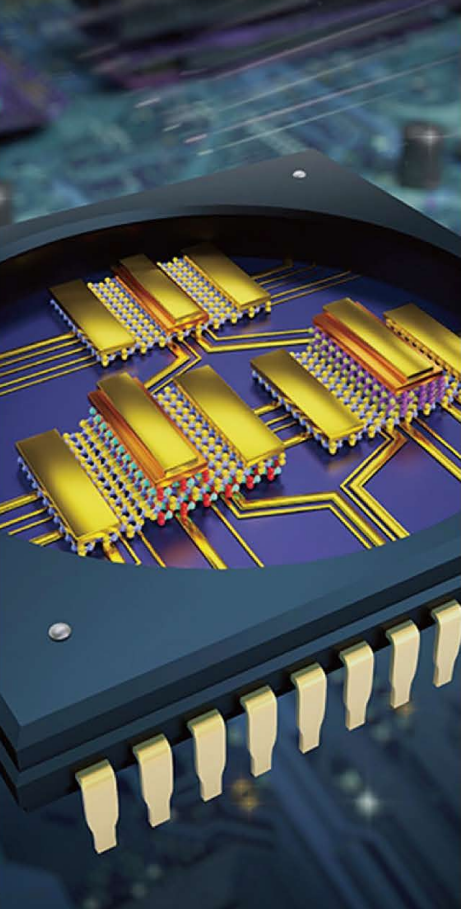
As one of the early players in this area, ZHANG Yue’s team has established a long-term schedule for exploring these materials. They look to combine 2D materials with silicon chips and eventually translate the innovations to industry.
“I believe that 2D materials and vdW heterostructures will find their place in optoelectronic devices and integrated circuits before long,” ZHANG Yue says.
Reference:
1.How 2D semiconductors could extend Moore’s law, Nature. 2019; 567: 169-170 https://www.nature.com/articles/d41586-019-00793-8
2.Near-ideal van der Waals rectifiers based on all-two-dimensional Schottky junctions. Nature Communications, 2021, 12, 1522https://www.nature.com/articles/s41467-021-21861-6
3. High-order superlattices by rolling up van der Waals heterostructures. Nature. 2021; 591(7850): 385 https://www.nature.com/articles/s41586-021-03338-0