colloidal Solution engineering for semiconductor electronic devices
Colloidal solution engineering is a potential low-cost fabrication of low-dimensional semiconductors based on chemical coordination and molecule ligands, constructing atomic scale electronic devices for next generation information technology
Atom-scale electronic devices and integration based on low-dimensional semiconductors have become a global priority for next-generation information technologies. “Yet, the sector is hampered by prohibitive fabrication costs and massive capital requirements; consequently, developing low-cost routes to atom-scale semiconductor materials and constructing advanced micro-/nano-electronic devices and systems is a core industry objective,” says TIAN Jianjun, Professor of University of Science and Technology Beijing.
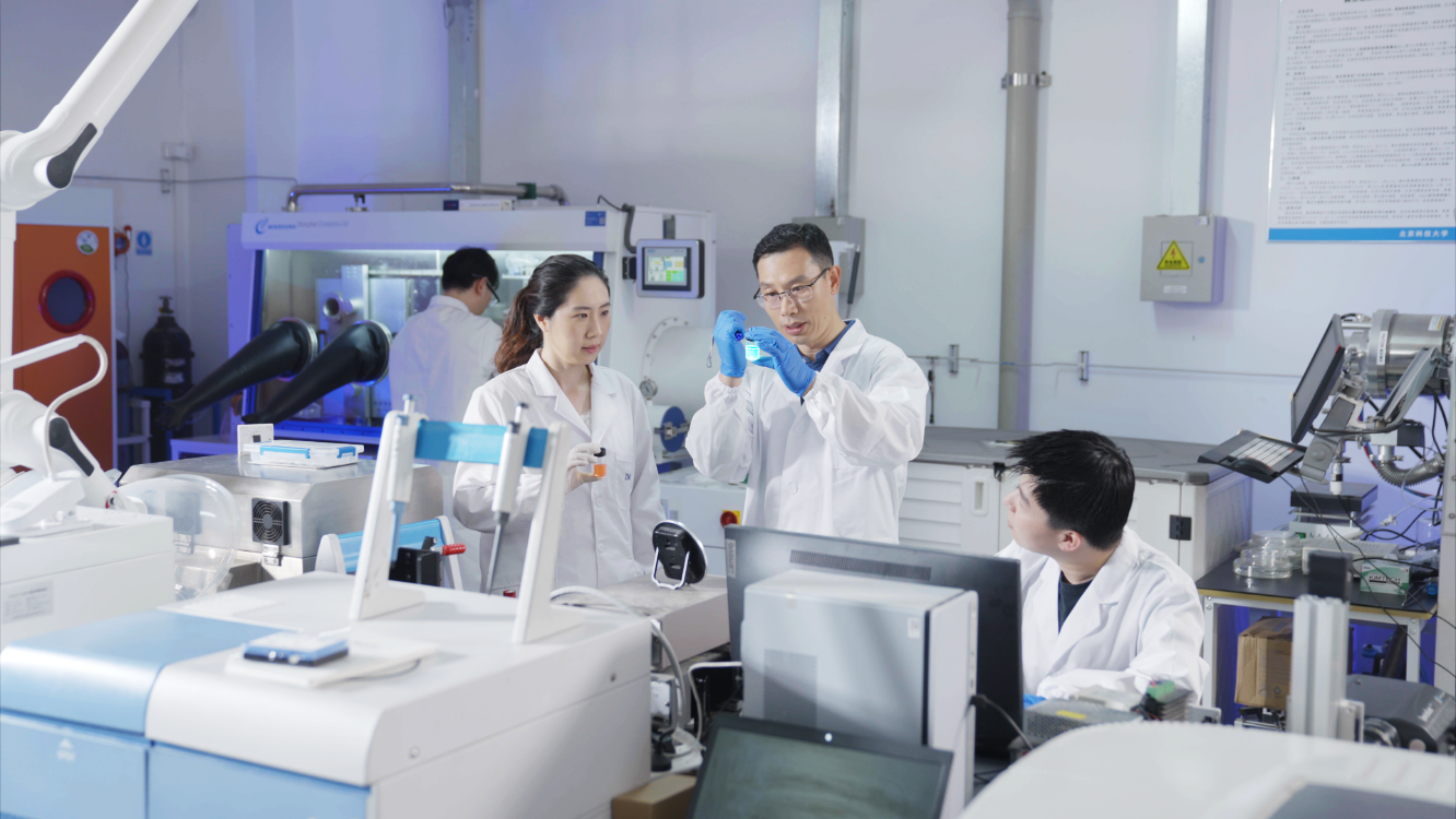
Over the past decade, TIAN’s team has concentrated on low-cost colloidal solution engineering of low-dimensional semiconductor thin films and nanocrystals to create high-performance electronic devices. Their sustained effort has yielded a series of major original breakthroughs, with key results published in journals such as Science1, and several technologies have already moved toward commercialization.
COLLOIDAL ORDINATION ENABLES SINGLE-CRYSTAL THIN FILMS
Fabricating semiconductor single-crystal thin films via colloidal solution engineering is notoriously difficult. “Anisotropic crystal growth and multidirectional nucleation suppress the formation of a continuous single-crystal film, yielding high defect densities and low carrier mobilities,” says Tian.
To overcome these obstacles, TIAN’s team has developed a multi-molecular coordination strategy that precisely steers crystal orientation during growth. Using this approach, they have successfully synthesized a series of oxide and halide single-crystal thin films and demonstrated their integration into high-performance electronic devices.
For example, the epitaxial single-crystal films of fluorite-structured bismuth oxide grown by this colloidal-solution route retain stable macroscopic ferroelectricity down to the atomic scale—an unprecedented 1 nm thickness—representing the highest ferroelectric performance yet achieved at this dimensional limit1. The halide semiconductor films with pushed carrier mobility to value approaching that of single-crystal have been achieved by colloidal-solution process2.
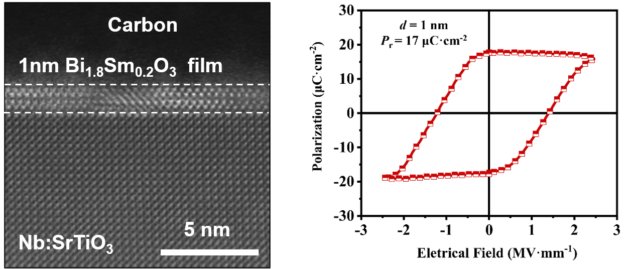
Atomic-scale (1 nm thickness) bismuth oxide film scanning transmission electron microscopy (left), and its ferroelectric hysteresis loops (right).
COLLOIDAL SEMICONDUCTOR NANOCRYSTALS
Colloidal semiconductor nanocrystals with strong quantum-confinement—commonly known as quantum dots—possess atom-like discrete energy levels that endow them with ultra-narrow spectral emission, exceptional color saturation, and an ultra-wide color gamut. “These attributes make them highly promising for high-definition displays and solid-state lighting applications” says TIAN.
Recently emerged halide semiconductor nanocrystals have attracted intense attention because they promise an even wider display color gamut. “Yet their high surface-defect density and poor stability remain critical bottlenecks” says TIAN.
To tackle these problems, TIAN’s team established a halide-ion-mediated Ostwald-ripening suppression route that affords precise control over nanocrystal growth, and introduced a design concept in which polar-molecule etching steers crystal orientation. These strategies have yielded a family of high-quality, strongly confined nanocrystals—quantum dots, quantum wells, and quantum wires alike.
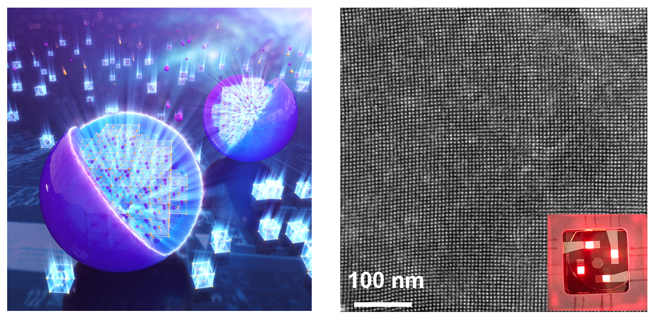
Quantum dots schematic diagram (left), quantum dots assembly superlattice film (right) and light-emitting diodes (inset).
Further, the team developed strongly chelating multidentate thiol ligands and a surface-etching-driven ligand-exchange technique that reconstruct the nanocrystal surface. By uncovering the Auger-recombination mechanism in diodes and its suppression pathways, they realized highly stable, optically superior pure-blue halide nanocrystal light-emitting diodes3–5. The work was highlighted by Nature Photonics6as delivering state-of-the-art performance in pure-blue emitters.
REFERENCES
[1] Yang, Q. et al. Science 379(6638), 1218-1224 (2023). https:/doi.org/10.1126/science.abm5134
[2] Yuan, J. et al. Adv. Funct. Mater. 47(32), 2209070 (2022). https:/doi.org/10.1002/adfm.202209070
[3] Bi, C. et al. Adv. Mater. 33(15), 2006722 (2021). https:/doi.org/10.1002/adma.202006722
[4] Zhang, M. et al. Angew. Chem. Int. Ed. 62(12), e202300149 (2023). https:/doi.org/10.1002/anie.202300149
[5] Zhang, M. et al. ACS Nano 19(7), 7283-7293 (2025). https:/doi.org/10.1021/acsnano.4c17654
[6] Woo, S. et al. Nat. Photonics 15(9), 630-634 (2021).
https://doi.org/10.1038/s41566-021-00863-2
图片材料