USTB is committed to building itself into a high-level research-oriented university
which attaches importance to novel scientific research and promotes independent innovation.
Recently, Professor Yue Zhang and Dr. Zheng Zhang’s research team from the School of Advanced Materials and Research Institute of Frontier Science and Technology at the University of Science and Technology Beijing (USTB) published a landmark paper in Nature Materials entitled:
“Two-dimensional Czochralski growth of single-crystal MoS₂.”
The first author of the paper is Dr. He Jiang.
Breakthrough in 2D Semiconductor Growth
Large-scale, high-quality two-dimensional transition metal dichalcogenides (TMDCs), such as molybdenum disulfide (MoS₂), are regarded as essential materials for next-generation semiconductor devices. However, achieving defect-free, wafer-scale growth of single-crystal MoS₂ has been a long-standing challenge.
The USTB team proposed a novel two-dimensional Czochralski (2DCZ) growth method, inspired by the classical crystal growth technique used for bulk semiconductors. This new approach enables the controllable growth of ultra-large, single-crystal MoS₂ domains with low defect density and excellent uniformity—marking an important step toward industrial-scale production of 2D semiconductors.
Innovative Growth Strategy
Traditional chemical vapor deposition (CVD) often results in polycrystalline films with grain boundaries that limit performance. In contrast, the 2DCZ method introduces a molten precursor spreading mechanism that allows MoS₂ to grow continuously in-plane. This process suppresses random nucleation, lowers defect density, and dramatically accelerates crystal growth—reaching a rate of 75 μm/s, far surpassing previous techniques.
Superior Material Quality
The single-crystal MoS₂ produced by this method demonstrated:
-Uniform atomic structure with defect density as low as 2.9 × 10¹² cm⁻²
-High electronic performance, with field-effect transistors (FETs) showing carrier mobility up to 105.4 cm² V⁻¹ s⁻¹
-Excellent scalability for wafer-level applications, enabling integration into high-performance devices
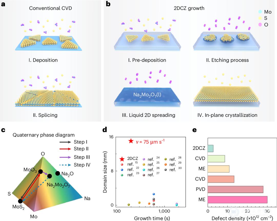
Figure 1 2DCZ crystallization of large-sized and high-quality MoS2 crystallites
Significance and Outlook
This achievement not only advances the fundamental understanding of 2D material growth but also provides a feasible route for large-area, defect-free, single-crystal TMDCs. The results hold great promise for next-generation semiconductors, optoelectronics, and flexible devices, accelerating the transition of 2D materials from the laboratory to industrial applications.